- 您现在的位置:买卖IC网 > Sheet目录313 > AT45DB081B-TI (Atmel)IC FLASH 8MBIT 20MHZ 28TSOP
�� �
�
�AT45DB081B�
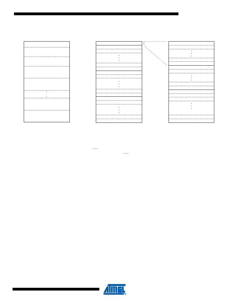
�Memory� Architecture� Diagram�
�SECTOR� ARCHITECTURE�
�BLOCK� ARCHITECTURE�
�PAGE� ARCHITECTURE�
�SECTOR� 0� =� 8� Pages�
�2112� bytes� (2K� +� 64)�
�SECTOR� 0�
�BLOCK� 0�
�BLOCK� 1�
�8� Pages�
�PAGE� 0�
�PAGE� 1�
�SECTOR� 1� =� 248� Pages�
�65,472� bytes� (62K� +� 1984)�
�SECTOR� 2� =� 256� Pages�
�BLOCK� 2�
�PAGE� 6�
�67,584� bytes� (64K� +� 2K)�
�SECTOR� 3� =� 512� Pages�
�135,168� bytes� (128K� +� 4K)�
�SECTOR� 4� =� 512� Pages�
�135,168� bytes� (128K� +� 4K)�
�SECTOR� 8� =� 512� Pages�
�135,168� bytes� (128K� +� 4K)�
�SECTOR� 9� =� 512� Pages�
�135,168� bytes� (128K� +� 4K)�
�BLOCK� 30�
�BLOCK� 31�
�BLOCK� 32�
�BLOCK� 33�
�BLOCK� 62�
�BLOCK� 63�
�BLOCK� 64�
�BLOCK� 65�
�BLOCK� 510�
�BLOCK� 511�
�Block� =� 2112� bytes�
�(2K� +� 64)�
�PAGE� 7�
�PAGE� 8�
�PAGE� 9�
�PAGE� 14�
�PAGE� 15�
�PAGE� 16�
�PAGE� 17�
�PAGE� 18�
�PAGE� 4093�
�PAGE� 4094�
�PAGE� 4095�
�Page� =� 264� bytes�
�(256� +� 8)�
�Device�
�Operation�
�Read� Commands�
�The� device� operation� is� controlled� by� instructions� from� the� host� processor.� The� list� of� instructions�
�and� their� associated� opcodes� are� contained� in� Tables� 1� through� 4.� A� valid� instruction� starts� with�
�the� falling� edge� of� CS� followed� by� the� appropriate� 8-bit� opcode� and� the� desired� buffer� or� main�
�memory� address� location.� While� the� CS� pin� is� low,� toggling� the� SCK� pin� controls� the� loading� of�
�the� opcode� and� the� desired� buffer� or� main� memory� address� location� through� the� SI� (serial� input)�
�pin.� All� instructions,� addresses� and� data� are� transferred� with� the� most� significant� bit� (MSB)� first.�
�Buffer� addressing� is� referenced� in� the� datasheet� using� the� terminology� BFA8� -� BFA0� to� denote�
�the� nine� address� bits� required� to� designate� a� byte� address� within� a� buffer.� Main� memory�
�addressing� is� referenced� using� the� terminology� PA11� -� PA0� and� BA8� -� BA0� where� PA11� -� PA0�
�denotes� the� 12� address� bits� required� to� designate� a� page� address� and� BA8� -� BA0� denotes� the�
�nine� address� bits� required� to� designate� a� byte� address� within� the� page.�
�By� specifying� the� appropriate� opcode,� data� can� be� read� from� the� main� memory� or� from� either�
�one� of� the� two� data� buffers.� The� DataFlash� supports� two� categories� of� read� modes� in� relation� to�
�the� SCK� signal.� The� differences� between� the� modes� are� in� respect� to� the� inactive� state� of� the�
�SCK� signal� as� well� as� which� clock� cycle� data� will� begin� to� be� output.� The� two� categories,� which�
�are� comprised� of� four� modes� total,� are� defined� as� Inactive� Clock� Polarity� Low� or� Inactive� Clock�
�Polarity� High� and� SPI� Mode� 0� or� SPI� Mode� 3.� A� separate� opcode� (refer� to� <blue>Table� 1� on�
�page� 10� for� a� complete� list)� is� used� to� select� which� category� will� be� used� for� reading.� Please�
�refer� to� the� “Detailed� Bit-level� Read� Timing”� diagrams� in� this� datasheet� for� details� on� the� clock�
�cycle� sequences� for� each� mode.�
�CONTINUOUS� ARRAY� READ:� By� supplying� an� initial� starting� address� for� the� main� memory�
�array,� the� Continuous� Array� Read� command� can� be� utilized� to� sequentially� read� a� continuous�
�stream� of� data� from� the� device� by� simply� providing� a� clock� signal;� no� additional� addressing�
�information� or� control� signals� need� to� be� provided.� The� DataFlash� incorporates� an� internal�
�address� counter� that� will� automatically� increment� on� every� clock� cycle,� allowing� one� continuous�
�read� operation� without� the� need� of� additional� address� sequences.� To� perform� a� continuous� read,�
�an� opcode� of� 68H� or� E8H� must� be� clocked� into� the� device� followed� by� 24� address� bits� and� 32�
�don’t� care� bits.� The� first� three� bits� of� the� 24-bit� address� sequence� are� reserved� for� upward� and�
�3�
�2225J–DFLSH–2/08�
�发布紧急采购,3分钟左右您将得到回复。
相关PDF资料
AT45DB161B-TI
IC FLASH 16MBIT 20MHZ 28TSOP
AT45DB321-TC
IC FLASH 32MBIT 13MHZ 32TSOP
AT45DB321B-TI
IC FLASH 32MBIT 20MHZ 32TSOP
AT45DB321C-TC
IC FLASH 32MBIT 40MHZ 28TSOP
AT45DB642-TC
IC FLASH 64MBIT 20MHZ 40TSOP
AT88CK9000-8TH
CRYPTO PROGRAMMER BOARD 8-TSSOP
AT88SC12816C-MJ
IC EEPROM 128KBIT 1.5MHZ M2J
AT88SC25616C-MJ
IC EEPROM 256BIT 1.5MHZ M2J
相关代理商/技术参数
AT45DB081B-TI-2.5
功能描述:闪存 8M SERIAL 2.7V - 2.5V IND TEMP RoHS:否 制造商:ON Semiconductor 数据总线宽度:1 bit 存储类型:Flash 存储容量:2 MB 结构:256 K x 8 定时类型: 接口类型:SPI 访问时间: 电源电压-最大:3.6 V 电源电压-最小:2.3 V 最大工作电流:15 mA 工作温度:- 40 C to + 85 C 安装风格:SMD/SMT 封装 / 箱体: 封装:Reel
AT45DB081B-TU
功能描述:闪存 8M 28 I/O Pins SPI 264B 2.7V RoHS:否 制造商:ON Semiconductor 数据总线宽度:1 bit 存储类型:Flash 存储容量:2 MB 结构:256 K x 8 定时类型: 接口类型:SPI 访问时间: 电源电压-最大:3.6 V 电源电压-最小:2.3 V 最大工作电流:15 mA 工作温度:- 40 C to + 85 C 安装风格:SMD/SMT 封装 / 箱体: 封装:Reel
AT45DB081D
制造商:ATMEL 制造商全称:ATMEL Corporation 功能描述:8-megabit 2.5-volt or 2.7-volt DataFlash
AT45DB081D_07
制造商:ATMEL 制造商全称:ATMEL Corporation 功能描述:8-megabit 2.5-volt or 2.7-volt DataFlash
AT45DB081D_08
制造商:ATMEL 制造商全称:ATMEL Corporation 功能描述:8-megabit 2.5-volt or 2.7-volt DataFlash
AT45DB081D_09
制造商:ATMEL 制造商全称:ATMEL Corporation 功能描述:8-megabit 2.5-volt or 2.7-volt DataFlash
AT45DB081D_13
制造商:AD 制造商全称:Analog Devices 功能描述:8-megabit 2.5V or 2.7V DataFlash
AT45DB081D-DWF
制造商:Adesto Technologies Corporation 功能描述:WHOLE WAFER, NO BACKGRIND - Gel-pak, waffle pack, wafer, diced wafer on film